Currently, there are more than 100 companies all over the world building ASICs (Application Specific Integrated Circuit) or SOC’s (System on Chip) targeted towards deep learning applications. There is a long list of companies here. In addition to these startup big companies like Google (TPU), Facebook, Amazon (Inferentia), Tesla etc are all developing custom ASIC’s for deep learning training and inference. These can be categorized into two types —
- Training and Inference — These ASIC’s are designed to handle both training the deep neural network and also performing inference. Training a large neural network like Resnet-50 is a much more compute-intensive task involving gradient descent and back-propagation. Compared to training inference is very simple and requires less computation. NVidia GPU’s, which are most popular today for deep learning, can do both training and inference. Some other examples are Graphcore IPU, Google TPU V3, Cerebras, etc. OpenAI has great analysis showing the recent increase in compute required for training large networks.
- Inference — These ASICs are designed to run DNN’s (Deep neural networks) which have been trained on GPU or other ASIC and then trained network is modified (quantized, pruned etc) to run on a different ASIC (like Google Coral Edge TPU, NVidia Jetson Nano). Most people say that the market for deep learning inference is much bigger than the training. Even very small microcontrollers (MCU’s) based on ARM Cortex-M0, M3, M4 etc can do inference as shown by the TensorFlow Lite team.

AI Landscape by Shan Tang : Source
Making any chip (ASIC, SOC etc) is a costly, difficult and lengthy process typically done by teams of 10 to 1000’s of people depending on the size and complexity of the chip. Here I am only providing a brief overview specific to deep learning inference accelerator. If you have already designed chips you may find this too simple. If you are still interested, read on! If you like it share and 👏 .
Architecture of Existing ASIC’s
Lets first look at the high-level architecture of some of the accelerators currently being developed.
Habana Goya — Habana labs is a start-up which is developing separate chips for training — Gaudi and inference — Goya.
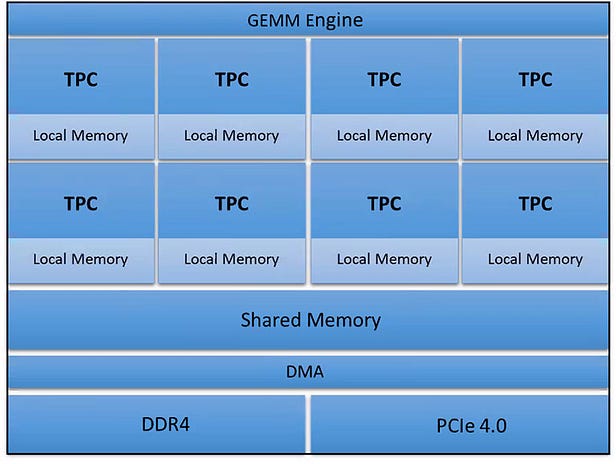
Habana Goya High-Level Architecture: Source
GEMM Engine — General matrix and multiply Engine. Matrix multiplication is the core operation in all DNN’s — convolution can be represented as matrix multiplication and fully connected layers are straight forward matrix multiplication.
TPC — Tensor processing Core — this is a block which actually performs the multiplication or multiply and accumulate (MAC) operation.
Local Memory and Shared Memory — These are both some form of cache commonly implemented using SRAM (Static Random Access Memory) and Register file (also type of static volatile memory just less dense than SRAM).
Eyeriss — The Eyeriss team from MIT has been working on deep learning inference accelerators and have published several papers about their two chips namely Eyeriss V1 and V2. You can find good tutorials here.

Eyeriss V2 top-level architecture: Source
Nvidia Deep Learning Accelerator (NVDLA)

NVDLA : Source
Dataflow Architecture — Dataflow architectures has been in research since the 1970s at least. Wave Computing came up with Dataflow processing unit (DPU) to accelerate training of DNN’s. Hailo also uses some form of dataflow architecture.
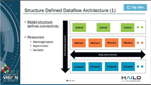
Hailo — Embedded Vision Summit — Source
Gyrfalcon — They have already released some chips like the Lightspeeur 2801S targeted towards low power Edge AI applications.

Matrix Processing Engine (MPE) — Source
Google TPU also has a systolic data flow engine.
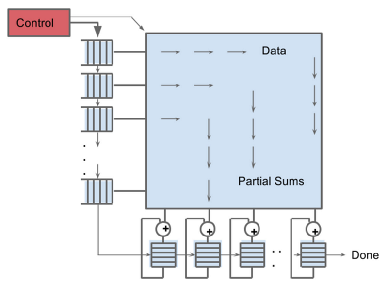
Matrix Multiplier on TPU — Source

TPU Floor plan — Source
Unified Buffer — This is basically local memory/cache probably implemented using SRAM.
DRAM — These are interfaces to access external DRAM, with two of them you can access 2x the data.
Key Blocks
Based on some of the above examples we can say that below are the key components required to make a deep learning inference accelerator. Also, we will only focus on 8-bit inference engine which has been shown to be good enough for many applications.
Matrix multiplication Unit — This is referred by different names like TPC (Tensor processing core), PE, etc. GEMM is the core computation involved in DNN’s, to learn more about GEMM read this great post.
SRAM — This is the local memory used to store the weights or intermediate outputs/activations.

Data movement Energy Vs Compute — Source — Efficient Processing of Deep Neural Networks: A Tutorial and Survey
To reduce energy consumption the memory should be located as close as possible to the processing unit and should be accessed as little as possible.
Interconnect/Fabric — This is the logic which connects all the different processing units and memory so that output from one layer or block can be transferred to the next block. Also referred to as Network on Chip (NoC).
Interfaces (DDR, PCIE) — These blocks are needed to connect to external memory (DRAM) and an external processor.
Controller — This can be a RISC-V or ARM processor or custom logic which is used to control and communicate with all the other blocks and the external processor.
Architecture and Instruction Set
If we look at all the architectures we will see memory is always placed as close as possible to the compute. The reason is that moving data consumes more energy than compute. Let’s look at the computation and memory involved in AlexNet architecture, which broke the ImageNet record in 2012 —
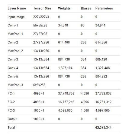
AlexNet Layers and Parameter — Source
AlexNet consists of 5 Constitutional layers and 3 fully connected layers. The total number of parameters/weights for AlexNet is around 62 million. Let's say after weight quantization each weight is stored as an 8-bit value so if we want to keep all the weights in on-chip memory it would require at least 62 MB of SRAM or 62*8 Mega-bits = 496 Million SRAM cells. If we use the 6T (six transistor) SRAM cell just the memory would require — 496M*6~2.9 Billion transistors. So while deciding architecture we have to keep in mind which DNN architectures we can support without keeping weights off-chip (which increases power consumption). For this reason lot of startups demonstrate using newer architectures like MobileNetV2 which use much fewer parameters and less compute, for example, one checkpoint of MobileNetV2 with Top-5 accuracy of 92.5% on ImageNet has only 6.06M parameters and performs 582M MACs (multiply and accumulate) operations during single image inference.

Accuracy Vs Model Size — Source
Weight pruning is another technique which can be used to reduce the model size (hence memory footprint). See results for model compression.
MobileNetV2 uses depthwise separable convolutions which are different from traditional convolution so the accelerator architecture has to be flexible enough so that if researchers come up with different operations they can still be represented in terms of the instruction set available on the accelerator.
We can come up with a very simple set of instructions for our simple accelerator like —
- Load Data — Takes source and destination address
- MAC (Multiply and accumulate) — Assumes data is already in the local register.
- Store result — Store the intermediate result
- PAD — To add zeros
Compilers for Hardware Accelerators
Compilers convert the high-level code written in python using PyTorch or Tensorflow to the instruction set for the specific chip. Below are some of the frameworks in development/use to work with these custom ASIC’s. This process can be very hard and complicated because different ASIC’s support different instruction sets and if the compiler doesn’t generate optimized code then you may not be taking full advantage of the capabilities of the ASIC.
Facebook Glow — Habana labs has developed a backend for their ASIC using the Glow framework.
TVM — This is an open-source deep learning compiler stack started by researchers at the University of Washington. The TVM framework also includes Versatile Tensor Accelerator (VTA) which is a programmable standalone accelerator. Amazon Sagemaker Neo uses TVM to compile deep learning models and deploy on different hardware.
TensorFlow MLIR — MLIR is the compiler infrastructure from Google for TensorFlow and has been recently been made part of the LLVM project.
Intel ngraph — This was developed by Nervana and used for the Nervana/Intel deep learning accelerators.
EDA Tools and High-Level Synthesis
Chisel — Chisel is hardware construction/description language initially developed by researchers at Berkeley. It's actually written in Scala and is used for the design of many RISC-V based processors.
Synthesis, Timing and Layout — RTL Synthesis is the process of converting high-level code written in Verilog/VHDL etc to logic gates. Timing tools use the pre- and post-layout delay information of the logic gates and routing to make sure the design is correct. In sequential design, everything happens with respect to the clock edge so timing is very important. Layout tools generate the layout from the synthesized netlist. Synopsys (Design Compiler, PrimeTime) and Cadence tools are most commonly used for these steps.
High-Level Synthesis (HLS) — HLS refers to the process when the hardware is described in a high-level language like C/C++ etc and then converted to a RTL (Register transfer level) language like VHDL/Verilog. There is even a python package http://www.myhdl.org/ — to convert python code to Verilog or VHDL. Cadence has commercial tools which support C/C++ etc, these tools can be very helpful for custom designs. Google used Mentor Graphics Catapult HLS tool to develop the WebM decompression IP.
Available IP
Now that we have identified the key blocks needed, let's look at what existing IP we use (free or paid).
Nvidia Deep Learning Accelerator (NVDLA) — NVDLA is a free and open architecture released by Nvidia for the design of deep learning inference accelerators. The source code, drivers, documentation etc are available on GitHub.
SRAM — Different types of SRAM IP — Single port, dual port, lower power, high speed etc for different process nodes is available from Synopsys and others. Typically they provide a SRAM compiler which is used to generate specific SRAM block as per the chip requirements.
Register File — This IP is also available from Synopsys and various types of logic standard cells.
Interconnect/Fabric/NoC — One of the options for this IP is Arteris, they have the FlexNoC AI Package targeted towards deep learning accelerators.
Processors — Various RISC-V processor cores are available for free. Even ARM gives licenses to startups for free or very low upfront cost. ARM Ethos NPUs are specially designed for neural networks — Ethos N37, N57, N77.

AMR Ethos NPU — Source
Cadence Tensilica DNA 100 — Cadence provides IP which can be configured from 0.5 to 100’s of TMAC operations depending on the application/industry we are targeting.
There are lots of other IP available so my advice is to look for already tested IP from companies like ARM, Ceva, NXP etc before designing your own.
Design Process
There are a lot of resources (books, lectures etc) available on ASIC design flow, digital design process etc so I will not cover it.

ASIC Flow from Wikipedia — Source
Foundries and Process technology
The manufacturing of chips is done is huge fabs (fabrication plants or foundries) and currently, there are very few companies like Intel, Samsung, Texas Instruments, NXP etc which own their own fabs. Even huge companies like Qualcomm, AMD etc use external foundries and all such companies are called fabless. Below are some of the biggest semiconductor foundries
TSMC (Taiwan Semiconductor manufacturing company) — TSMC is the worlds largest foundry and makes chips for companies like Qualcomm, Apple, etc. It can be challenging for small startups to manufacture at TSMC because most of their manufacturing capacity is used by big companies.
UMC (United Microelectronics Corporation) — UMC also works with a large number of customers including small startups. Currently, the smallest process available at UMC is 14nm.
There are several other foundries like Global foundry, Samsung foundry, etc
Process Selection
Cross-section of two transistors in a CMOS gate, in an N-well CMOS process
IC manufacturing processes are measured by the size of of the transistors and the width of the metal connections. For a long time, the process dimensions have been going down (Moore’s law) and that’s modern IC contain more and more transistors every year (this used to be governed by Moore’s law). Currently, the most advanced process node is 7nm and products using 7nm process were only launched in 2019. So most of the products are currently using chips made using 14nm/16nm process. The more advanced the process the more expensive it's going to be hence most small startups will initially use a slightly older process to keeps costs low. Many of the startups developing deep learning accelerators are using 28nm processor or, in some cases, even 40nm process. Leakage is a big concern in modern processes and can contribute to significant power consumption if the chip is not designed properly.
Simple Cost Estimation
Wafer costs depend on the process node and various other things like number of processing steps (layers used). The cost can vary from around thousand dollars for relatively older processes to several thousand of dollars for the latest process node and depends a lot of how many wafers one is buying etc.
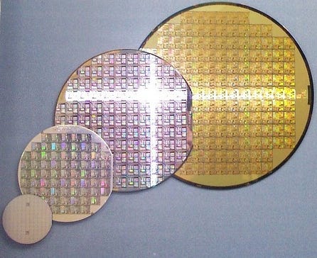
CMOS Wafer — Source
Most foundries produce 300 mm (~12 inch) diameter wafers for the digital processes. Let do simple calculation of die cost for a 12 inch wafer
Total Area ~ π * r ² (r = radius of wafer) ~ 70,650 mm²
Total Wafer Cost~$1000 (Just used for example)
Die Area ~ 10 mm x 10 mm ~ 100 mm² ( TPU V1 Die Size ~ 331 mm², SRAM Cell in 32 nm area ~ 0.18 um²)
Dies per wafer ~ 70,650 / 100 ~ 706 (Actually less due to edge defects etc)
Actually good dies with 95% yield ~ 0.95 * 706 ~ 670
Single Die Cost ~ $1000/670 ~ $1.5
Packaging and testing also add to the final cost.
This is a huge field and this post only touched the surface of some of these topics. There are so many other things to cover likeFPGA for deep learning, layout, testing, yield, low power design, etc. I may write another post if people like this one.
I’m passionate about building production machine learning systems to solve challenging real-world problems. I’m actively looking for ML/AI engineer positions, and you can contact mehere.
Links
Stanford CS 271 — Hardware Accelerators for Machine Learning
Plasticine and Spatial
See also DEEP DIVIDES BETWEEN AI CHIP STARTUPS, DEVELOPERS
